- English
- Español
- Português
- русский
- Français
- 日本語
- Deutsch
- tiếng Việt
- Italiano
- Nederlands
- ภาษาไทย
- Polski
- 한국어
- Svenska
- magyar
- Malay
- বাংলা ভাষার
- Dansk
- Suomi
- हिन्दी
- Pilipino
- Türkçe
- Gaeilge
- العربية
- Indonesia
- Norsk
- تمل
- český
- ελληνικά
- український
- Javanese
- فارسی
- தமிழ்
- తెలుగు
- नेपाली
- Burmese
- български
- ລາວ
- Latine
- Қазақша
- Euskal
- Azərbaycan
- Slovenský jazyk
- Македонски
- Lietuvos
- Eesti Keel
- Română
- Slovenski
- मराठी
- Srpski језик


 coating")

Wafeltje
Wafeltje
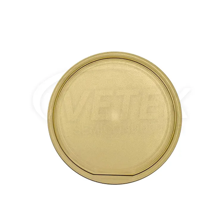
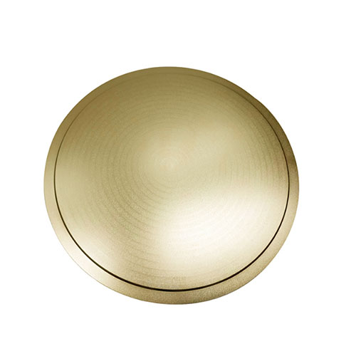
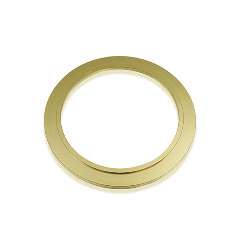
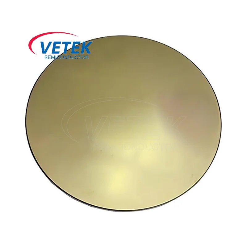
Wafelsubstraatis een wafer gemaakt van halfgeleider monokristallijn materiaal. Het substraat kan direct het wafelproductieproces ingaan om halfgeleiderapparaten te produceren, of het kan worden verwerkt via een epitaxiaal proces om epitaxiale wafels te produceren.
Wafersubstraat, als de fundamentele ondersteunende structuur van halfgeleiderapparaten, heeft een directe invloed op de prestaties en stabiliteit van de apparaten. Als "basis" voor de productie van halfgeleiderapparaten moet een reeks productieprocessen zoals dunne-filmgroei en lithografie op het substraat worden uitgevoerd.
Samenvatting van substraattypen:
●Eenkristal siliciumwafel: momenteel het meest voorkomende substraatmateriaal, dat veel wordt gebruikt bij de vervaardiging van geïntegreerde schakelingen (IC's), microprocessors, geheugens, MEMS-apparaten, stroomapparaten, enz.;
●SOI-substraat: gebruikt voor hoogwaardige geïntegreerde schakelingen met laag vermogen, zoals hoogfrequente analoge en digitale schakelingen, RF-apparaten en energiebeheerchips;

●Samengestelde halfgeleidersubstraten: Galliumarsenidesubstraat (GaAs): microgolf- en millimetergolfcommunicatieapparatuur, enz. Galliumnitridesubstraat (GaN): gebruikt voor RF-vermogensversterkers, HEMT, enz.Siliciumcarbidesubstraat (SiC): gebruikt voor elektrische voertuigen, stroomomvormers en andere energieapparaten. Indiumfosfidesubstraat (InP): gebruikt voor lasers, fotodetectoren, enz.;

●Saffier substraat: gebruikt voor LED-productie, RFIC (radiofrequentie-geïntegreerde schakeling), enz.;
Vetek Semiconductor is een professionele leverancier van SiC-substraten en SOI-substraten in China. Ons4H semi-isolerend SiC-substraatEn4H semi-isolerend type SiC-substraatworden veel gebruikt in belangrijke componenten van halfgeleiderproductieapparatuur.
Vetek Semiconductor streeft ernaar geavanceerde en aanpasbare Wafer Substrate-producten en technische oplossingen met verschillende specificaties voor de halfgeleiderindustrie te leveren. Wij kijken er oprecht naar uit om uw leverancier in China te worden.
ALD
ALD
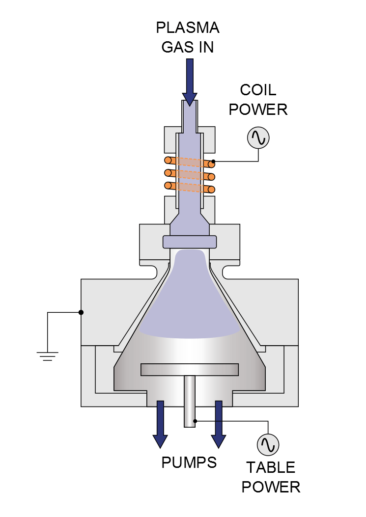
Thin film preparation processes can be divided into two categories according to their film forming methods: physical vapor deposition (PVD) and chemical vapor deposition (CVD), of which CVD process equipment accounts for a higher proportion. Atomic layer deposition (ALD) is one of the chemical vapor deposition (CVD).
Atomic layer deposition technology (Atomic Layer Deposition, referred to as ALD) is a vacuum coating process that forms a thin film on the surface of a substrate layer by layer in the form of a single atomic layer. ALD technology is currently being widely adopted by the semiconductor industry.
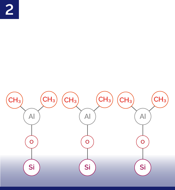
Atomic layer deposition process:
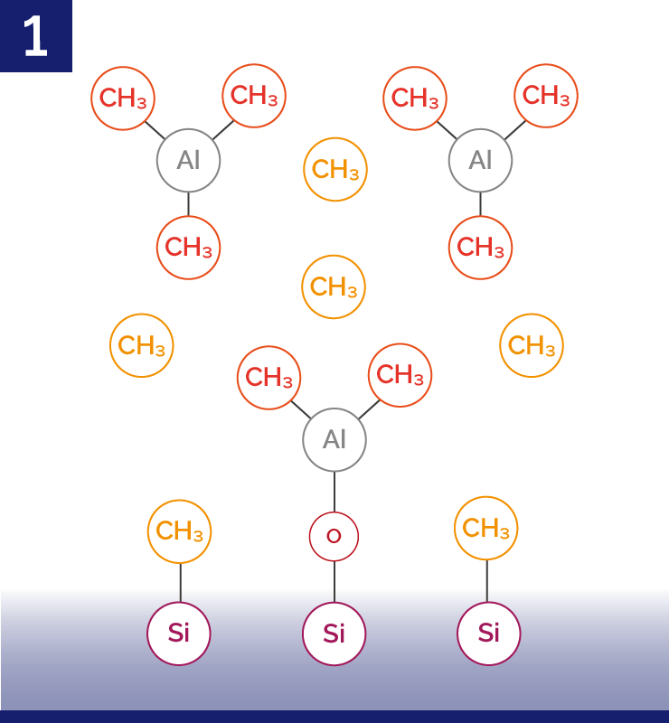
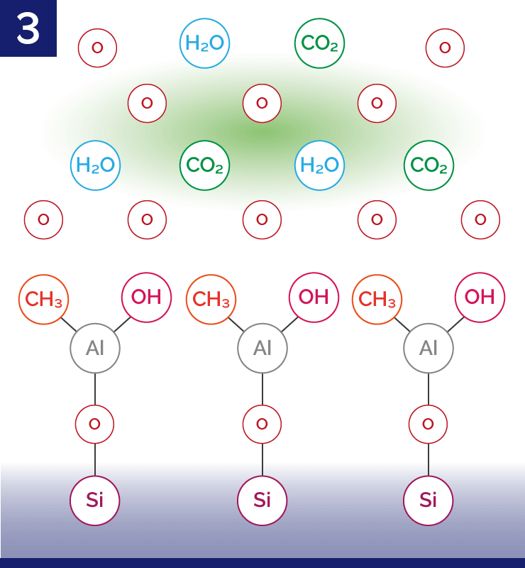
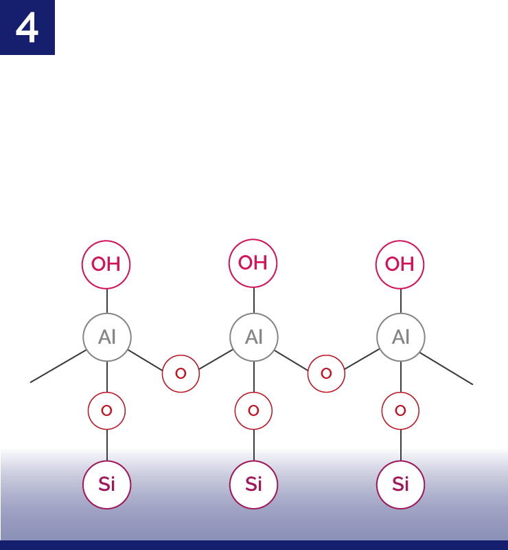
Atomic layer deposition usually includes a cycle of 4 steps, which is repeated as many times as needed to achieve the required deposition thickness. The following is an example of ALD of Al₂O₃, using precursor substances such as Al(CH₃) (TMA) and O₂.
Step 1) Add TMA precursor vapor to the substrate, TMA will adsorb on the substrate surface and react with it. By selecting appropriate precursor substances and parameters, the reaction will be self-limiting.
Step 2) Remove all residual precursors and reaction products.
Step 3) Low-damage remote plasma irradiation of the surface with reactive oxygen radicals oxidizes the surface and removes surface ligands, a reaction that is also self-limiting due to the limited number of surface ligands.
Step 4) Reaction products are removed from the chamber.
Only step 3 differs between thermal and plasma processes, with H₂O being used in thermal processes and O₂ plasma being used in plasma processes. Since the ALD process deposits (sub)-inch-thick films per cycle, the deposition process can be controlled at the atomic scale.
Highlights of Atomic Layer Deposition (ALD):
1) Grow high-quality thin films with extreme thickness accuracy, and only grow a single atomic layer at a time
2) Wafer thickness can reach 200 mm, with typical uniformity <±2%
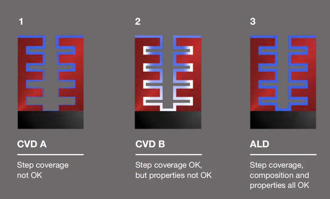
3) Excellent step coverage even in high aspect ratio structures
4) Highly fitted coverage
5) Low pinhole and particle levels
6) Low damage and low temperature process
7) Reduce nucleation delay
8) Applicable to a variety of materials and processes
Compared with traditional chemical vapor deposition (CVD) and physical vapor deposition (PVD), the advantages of ALD are excellent three-dimensional conformality, large-area film uniformity, and precise thickness control, etc. It is suitable for growing ultra-thin films on complex surface shapes and high aspect ratio structures. Therefore, it is widely applicable to substrates of different shapes and does not require control of reactant flow uniformity.
Comparison of the advantages and disadvantages of PVD technology, CVD technology and ALD technology:
|
PVD technology |
CVD technology |
ALD technology |
|
Faster deposition rate |
Average deposition rate |
Slower deposition rate |
|
Thicker film thickness, poor control of nano-level film thickness precision |
Medium film thickness (depends on the number of reaction cycles) |
Atomic-level film thickness |
|
The coating has a single directionality |
The coating has a single directionality |
Good uniformity of large-area film thickness |
|
Poor thickness uniformity |
Average step coverage |
Best step coverage |
|
Poor step coverage |
\ |
Dense film without pinholes |
Advantages of ALD technology compared to CVD technology (Source: ASM)
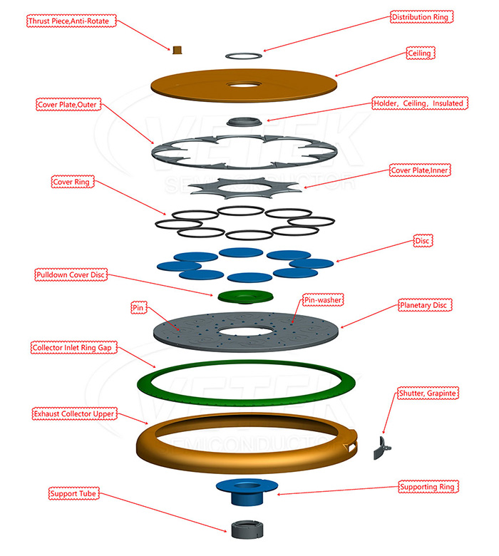
Vetek Semiconductor is a professional ALD Susceptor products supplier in China. Our ALD Susceptor, SiC coating ALD susceptor and ALD Planetary Susceptor are widely used in key components of semiconductor manufacturing equipment. Vetek Semiconductor is committed to providing advanced and customizable ALD Susceptor products and technical solutions of various specifications for the semiconductor industry. We sincerely look forward to becoming your supplier in China.
Uitgelichte producten
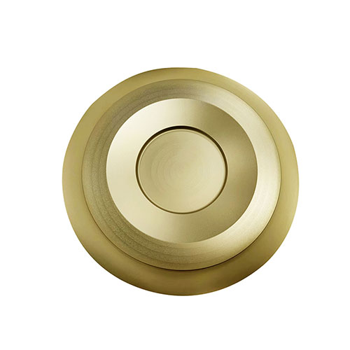
Massieve SiC schijfvormige douchekop
Keramische E-klauwplaat
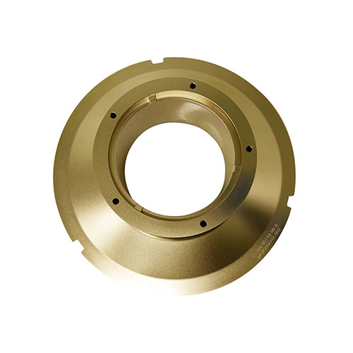
CVD SiC-gecoate wafelvathouder
Vat susceptor met CVD SiC-coating
CVD SiC-coating Wafer Epi Susceptor
Hyperpuur grafiet stijf vilt
Hoge zuiverheid Stijve vilten buis
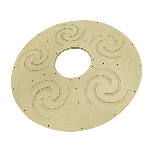
Grafiet susceptor met CVD SiC-coating
CVD SiC-coating Verwarmingselement
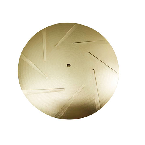
Grafiet roterende ontvanger
Zeer zuivere grafietring
SiC keramische afdichtring


Over ons
VeTek semiconductor Technology Co., LTD, opgericht in 2016, is een toonaangevende leverancier van geavanceerde coatingmaterialen voor de halfgeleiderindustrie. Onze oprichter, een voormalig expert van het Institute of Materials van de Chinese Academie van Wetenschappen, heeft het bedrijf opgericht met de nadruk op het ontwikkelen van geavanceerde oplossingen voor de industrie.
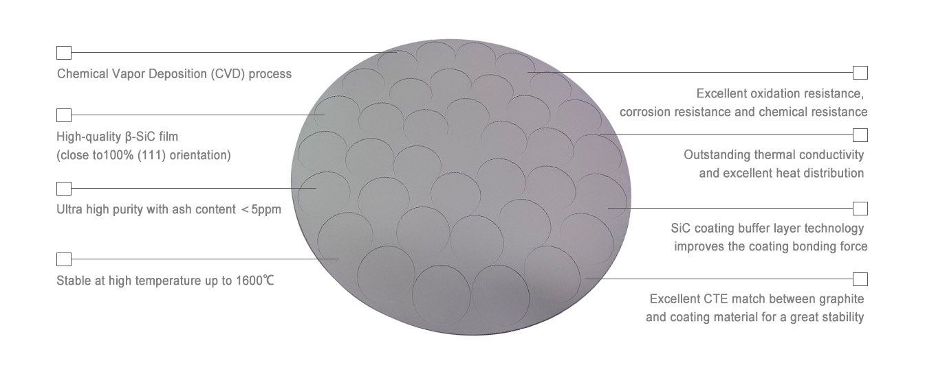
Ons belangrijkste productaanbod omvatCVD siliciumcarbide (SiC) coatings, tantaalcarbide (TaC) coatings, bulk SiC, SiC-poeders en zeer zuivere SiC-materialen. De belangrijkste producten zijn SiC-gecoate grafiet susceptor, voorverwarmringen, TaC-gecoate afleidingsring, halvemaanonderdelen, enz., De zuiverheid is lager dan 5 ppm en kan aan de eisen van de klant voldoen.
Ons belangrijkste productaanbod omvatCVD siliciumcarbide (SiC) coatings, tantaalcarbide (TaC) coatings, bulk SiC, SiC-poeders en zeer zuivere SiC-materialen. De belangrijkste producten zijn SiC-gecoate grafiet susceptor, voorverwarmringen, TaC-gecoate afleidingsring, halvemaanonderdelen, enz., De zuiverheid is lager dan 5 ppm en kan aan de eisen van de klant voldoen.

Nieuwe Producten
Nieuws

Halfgeleiderproces: Chemical Vapour Deposition (CVD)
Chemische dampafzetting (CVD) bij de productie van halfgeleiders wordt gebruikt om dunne-filmmaterialen in de kamer af te zetten, waaronder SiO2, SiN, enz., en veelgebruikte typen zijn onder meer PECVD en LPCVD. Door de temperatuur, druk en het type reactiegas aan te passen, bereikt CVD een hoge zuiverheid, uniformiteit en goede filmdekking om aan verschillende procesvereisten te voldoen.
Lees verder

Hoe het probleem van sinterscheuren in siliciumcarbide-keramiek oplossen? - VeTek-halfgeleider
Dit artikel beschrijft voornamelijk de brede toepassingsmogelijkheden van siliciumcarbidekeramiek. Het richt zich ook op de analyse van de oorzaken van sinterscheuren in siliciumcarbidekeramiek en de bijbehorende oplossingen.
Lees verder

Wat is stapgecontroleerde epitaxiale groei?
Lees verder

De problemen bij het etsproces
De etstechnologie bij de productie van halfgeleiders stuit vaak op problemen zoals belastingseffect, microgroefeffect en oplaadeffect, die de productkwaliteit beïnvloeden. Verbeteroplossingen omvatten het optimaliseren van de plasmadichtheid, het aanpassen van de reactiegassamenstelling, het verbeteren van de efficiëntie van het vacuümsysteem, het ontwerpen van een redelijke lithografie-indeling en het selecteren van geschikte etsmaskermaterialen en procesomstandigheden.
Lees verder

Wat is heetgeperst SiC-keramiek?
Heet persen sinteren is de belangrijkste methode voor het bereiden van hoogwaardige SiC-keramiek. Het proces van heetpersen sinteren omvat: het selecteren van zeer zuiver SiC-poeder, persen en vormen onder hoge temperatuur en hoge druk, en vervolgens sinteren. SiC-keramiek vervaardigd volgens deze methode heeft de voordelen van hoge zuiverheid en hoge dichtheid, en wordt veel gebruikt in slijpschijven en warmtebehandelingsapparatuur voor wafelverwerking.
Lees verder

Toepassing van op koolstof gebaseerde thermische veldmaterialen bij de kristalgroei van siliciumcarbide
De belangrijkste groeimethoden van siliciumcarbide (SiC) zijn onder meer PVT, TSSG en HTCVD, elk met duidelijke voordelen en uitdagingen. Op koolstof gebaseerde thermische veldmaterialen zoals isolatiesystemen, smeltkroezen, TaC-coatings en poreus grafiet verbeteren de kristalgroei door stabiliteit, thermische geleidbaarheid en zuiverheid te bieden, essentieel voor de nauwkeurige fabricage en toepassing van SiC.
Lees verder